


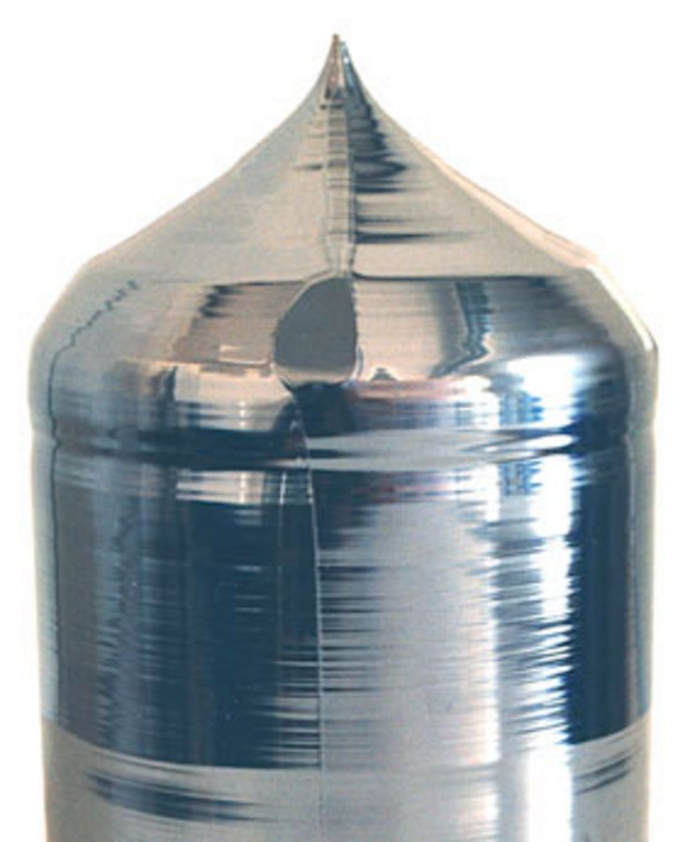
The Arithmeum is proud to be the first museum to present a notable advance in semiconductor technology: a silicon monocrystal with a diameter of 300 mm.
Silicon monocrystals comprise the basic element of chip production. Silicon is, after oxygen, the second most common chemical element on earth. In a lengthy process of highly developed and optimally coordinated production steps, sand is converted into a pure silicon monocrystal, from which a thin disc, a so-called wafer, is cut. In order for this wafer to be usable in semiconductor technology, it has to fulfill the following criteria: extreme chemical purity, nearly perfect crystal structure throughout, and a geometrically faultless surface.
The production chain begins with quartz sand from which raw silicon is extracted in an electrothermal process. This is converted to polysilicon via an intermediate step involving trichlorosilane. In a final step this is melted at a temperature of 1400 degrees C and a pure silicon monocrystal is grown by means of a tiny starter crystal. In the past, the largest silicon monocrystals had a diameter of up to 200 mm. A new, far more sophisticated production process now allows the formation of silicon monocrystals with a diameter of 300 mm. This increases the yield by a factor of 2.24, and up to 260 chips can now be placed on one wafer, which will accommodate around 10 billion transistors.
The firm Wacker Siltronic has, with the kind support of the firm Solar World AG, presented this 155 cm high silicon monocrystal with a diameter of 300 mm and a weight of 216 kg to the Arithmeum. This one monocrystal would yield 1000 wafers worth a sum total of 1.5 million dollars.